Transistor Radio Series – AF Power Amp Notes
I sought a low distortion, single supply, AF power amplifier
for my transistor radios. I’ll present my experiments, some musings, test
equipment and a reference to some wonderful books & their wise author.
Sadly, some amateur radio receiver builders diligently craft their RF stages,
but skimp on the PA audio stage. Actually — many commercial radio designers also do
this.
Why? This make
no sense. I’ve spent many hours learning how to make good audio circuits & concluded
long ago -- they’re much easier to design than high frequency circuits;
especially as you move into microwave & beyond. At AF, you
don’t need much test gear, nor oscilloscope bandwidth to produce a quality
home built AF amplifier. Parts cost little — plus design books and web sites illustrating best practices seem abundant.
Still, many cave into running the LM386 (a good part) without due care --- or
they home brew something with discrete parts that “works” but makes a lot
of distortion even with modest input drive.
Many bad designs with 0 test measurements get copied and published on
the web; or in popular subscription quarterlies that serve QRP amateur radio audiences. If you look on the Web you’ll even find some crazy home brew audio
PA circuitry. For example, 1 builder put
an additional pair of NPN/PNP power followers on the output of an LM386 set in
high gain mode !
We’ve only got 2 secret weapons to make low distortion audio
PA's: global negative feedback (NFB), & to specifically design our circuitry to boost linearity at the local level. By far, NFB is the easier of the 2 — go ahead & use abundant NFB, but, of course, not to the point where you create an oscillator.
Amazingly, some discrete
component circuits shared on the Internet lack any form of of negative feedback! For many years
people like Wes Hayward extolled the virtues of NFB in amplifiers
from AF to RF. In 2018, our hobby should be measurement-driven. Dear reader, please promise me that you won't build any
discrete audio power amplifiers that lack NFB.
As radio designers, our single audio PA design goal proves exquisitely
simple: swing the largest possible, clean
sine wave between the power supply rails into a low-value resistor test load.
Further, we ought to reduce noise & common
mode hum, plus shape the PA audio bandwidth to suit our radio listening environment and /or speaker.
Enough commentary. Let's view some single DC supply audio
power amplifiers I built this Winter & Spring.
Amplifier 1: Discrete PA with a complimentary feedback pair for the finals.
Above — A non-inverting amplifier built with transistors I use everyday in my lab for DC to HF projects. Ever-popular, I adopted the classic 3 stage amp: differential transconductance input; voltage amplifier stage (VAS) ; plus some configuration of complimentary power output transistors.
For this amp, I copied many aspects of the Blameless Amplifier described by Douglas Self in his book Audio Power Amplifier Design, 6th edition by Focal Press. ISBN-13: 978-0240526133.
Of course, I converted it to single DC supply and also experimented with every resistor and many capacitor values in the pursuit of reduced distortion at lower singular, DC voltage. While I lack a total harmonic distortion analyzer, you can get pretty far with a low-distortion signal generator plus a DSO with an FFT. I enjoy a DSO + FFT with a 12-bit ADC and posted screen shots from that device.
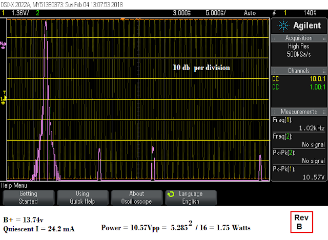
Above — An FFT of Amplifier 1 @ maximum clean average power. My DC power supply = 13.74 VDC and the load was a 8 Ω resistor bank. A properly built Blameless Amp with a negative/positive supply of at least +/- 15 VDC is capable of producing a total harmonic distortion of 0.0005% @ 1 KHz. You can't measure that low with a 'scope FFT, but my amp appears to have a THD less than 0.1 %.
Since we radio designers tend to use a 13.8 VDC DC supply (or slightly less), we'll incur slightly more distortion than the higher voltage, split DC supply designs.
The theoretical maximum possible sine wave output without distortion is slightly < 3 Watts with a 13.75 volt power supply. That is about 2 dB more than I got, but practically considering the saturation voltage of the output transistors plus the drop across the 1 ohm resistors then it seems unlikely I'd get more that 2.3 watts as a maximum before distortion starts climbing steeply due to clipping — only about 1 dB more.
Average power is calculated as follows:
For each AF power amp, I advance the signal generator's drive until the 2nd and subsequent harmonics take off. Then I back off the drive until the signal cleans up and declare that the maximum clean average power.
Above — An FFT with the Amp # 1 driven to produce 3.0 Vpp into the 8 Ω resistor. No real change in distortion. I'll briefly discuss each of the 3 PA stages. For comprehensive information, consult Doug Self's book.
Input:
A balanced differential transconductance amp exhibits better linearity than a single input transistor power amp. We enjoy cancellation of the 2nd harmonic and boosted common mode noise reduction. The input pair are best balanced with current mirrors and fed with a current source as shown.
The 120 Ω emitter degeneration resistors provided slightly less THD than when I applied 100 Ω resistors. Above 120 Ω, I ran into the law of diminishing returns.
VAS
The VAS is driven by an emitter follower to reduce effects of this BJTs intrinsic collector to base feedback. An alternate way is to cascode two BJTs for the same reason. The 100 pf cap back to the emitter follower exerts local feedback to stabilize + linearize the VAS at high frequency. Global feedback linearizes the VAS at low frequency.
The VAS current source receives local NFB from the input pair current source. The VAS collector sees an active collector load to further boost linearity. Doug Self devotes an entire chapter to the VAS in his PA design book.
Further, a 33p collector cap suppresses some higher order harmonic distortion.
Finals
Instead of complimentary emitter followers, I employed push-pull common emitter amps organized as complimentary feedback pairs. Collector output stages seem attractive, but pose greater difficultly to achieve low distortion because they're very sensitive to individual output and driver transistor characteristics such as beta. You can even arrange the finals to exhibit gain, but a gain of 1 gave the best distortion profile.
I chose this output topology to get its output signal swinging as close to the DC supply rails as possible ( between 0 and 13.75 VDC ). To get this you must depart from the
standard complimentary pair of emitter followers. In these, the collector-to-emitter saturation voltage plus VBE keep you from getting close to the rails. Thus, I felt pleased to get 1.75 W output in a relatively low voltage, single DC supply PA circuit.
The 330 Ω resistors set a low drive impedance into the output transistors. I tested other values and settled with these
This PA sounds great in a receiver. Cranked to ear splitting volumes into a 8 Ω speaker, strong, thumping Morse code signals never clip the PA stage. Bliss!
You might argue that this amp uses too many transistors? My reply -- what good PA doesn't. Check out the schematic of your favorite op-amp. Transistors abound. Designers use BJTs as amplifiers + followers — and for current sources/mirrors, etc.; just like Amplifier 1 does. Transistors don't cost much these days and if you want to make a discrete PA, good for you. Discrete PAs are 1 of the last things left that can't be better built within an IC.

Above — A photo of Amplifier 1. You need heat sinks when pushing > 1 Watt continuously on the test bench. Mine were purchased on eBay for low cost and free shipping.
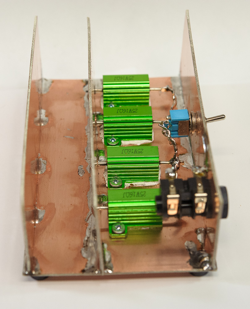
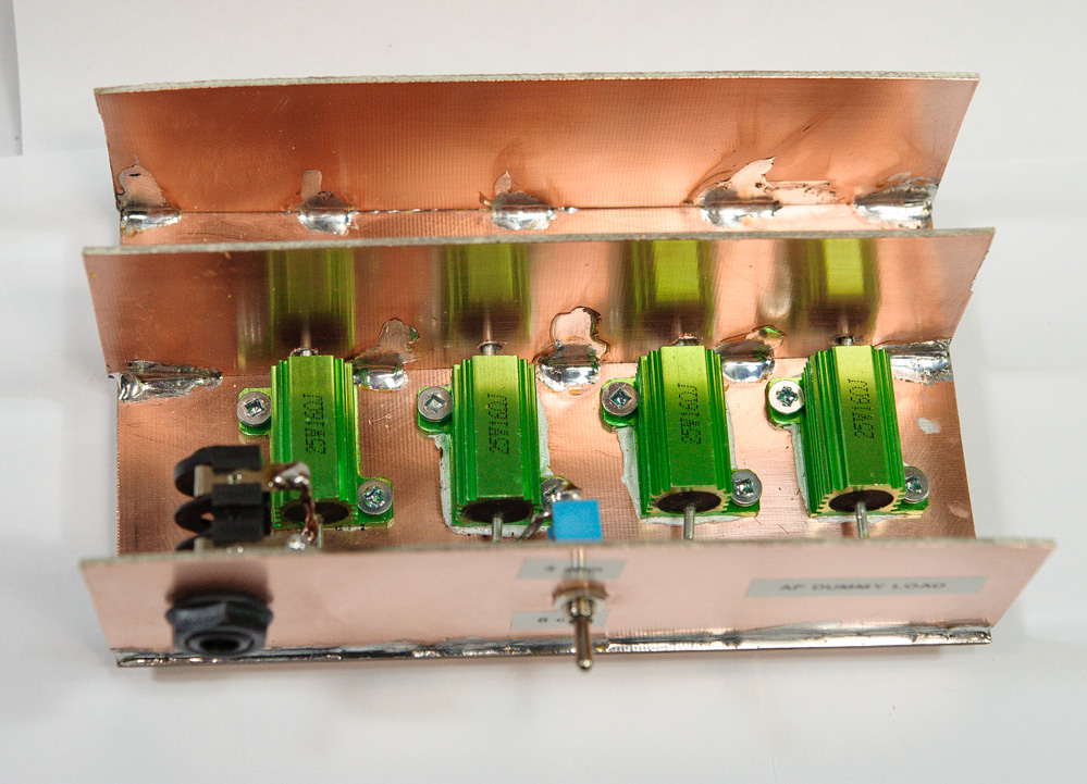
Above — 1 of the resistor loads I employed for these experiments. I've got several. This photo shows four 1 Watt resistors soldered in parallel to give 8 Ω. As I recall, the values were 33, 29, 27 and 27 which gave a measured 8 Ω. These will heat up when driving the amp near peak average power for any length of time.
Above — To set the bias for the finals, adjust the 1K trimmer pot on the VBE multiplier to 1.1 VDC. That is across points A and B [ blue color font within red squares in the Amplifier 1 schematic]. Then you can slightly trim this voltage as needed. For all intents, 1.1 to 1.2 VDC with no input signal works great and gives a total stage quiescent current of around 24 mA.
Above — I can't recommend this book enough. I hesitate to use the term expert, but Douglas Self provides a tour de force in this book's expert 718 pages. He writes clever, humorous prose that's fun to read and just plain interesting.
Doug Self possess encyclopedic knowledge of all things Hi Fi audio. He includes 1 chapter just on distortion which covers from capacitor distortion to the kitchen sink. He covers every topic you ever thought about such as FETs versus BJTs and cascode VAS designs. I particularly enjoyed his writing about "fear of feedback" & subjectivism. He's a scientific 'to measure is to know' devotee and debunks many of the myths that prevail in the audio world. Get this book!
Amplifier 2: Discrete PA with a complimentary feedback pair for the finals.
Above — Amplifier 2 is the same as Amplifier 1, however, used common small-signal AF transistors with an Ft of ~100 MHz and two 1 Ω in parallel resistors on the final BJT emitters.
Above —FFT of Amplifier 2 pushed to 2.07 Watts. This is the highest average power I've ever got with a single-supply @ 13.7 VDC
An interesting event happened. I initially chose the MJE140/150 complimentary transistors as my finals. Sadly, they only could muster ~ 8.7 Vpp before they went into serious clipping. I replaced them with a BD139/140 pair and got the results shown above. The Ft of the MJE pair = ~ 30 MHz, while the BD139/140 pair Ft is
likely over 140 MHz.
However, the most likely reason is probably beta. The beta of the MJE transistors is likely lower; particularly at low collector to emitter voltages compared to the BD pair. Most often, the MJE transistors are used at much higher voltages. I will stick to the BD139/140 pair for single- supply AF power amps.
I should mention that all these power amps exhibit low gain. The purpose of the circuitry is to deliver the maximum clean signal into an 8 Ω speaker. This means heavy NFB. You can easily build up your small signal voltage with op-amps, or if you're a purist — with discrete voltage amplifiers. In a power amplifier, stout NFB lowers harmonic distortion, rejects noise on the DC supply rail and keeps the output impedance low.
Above — DSO shot of Amplifier 2 driven to 1.56 Watts with my bench
12.3 VDC supply. If you lack a DSO with FFT, then just design for the cleanest looking sine wave you can muster as seen above.
Above — Time Domain analysis @
2 KHz. Driven to 815 mW
Amplifier 3: Discrete PA with complimentary emitter-followers for the finals.
Above — Schematic of Amplifier 3. The finals == the
classic complimentary emitter follower pair also driven with emitter followers. The rest of the circuitry looks pretty much the same as Amplifiers 1 and 2.
Above — FFT of Amplifier 3. The emitter follower finals deliver improved THD compared to the Amplifier 1's complimentary pair where the output is taken from the BJT collector. However, you can't deliver the same maximal average power with plain emitter follower outputs. This is a beautiful, very stable amplifier.
Above — FFT of Amplifier 3 driven to 1.53 Watts, the 2nd harmonic is just starting to take off!
Above — FFT of Amplifier 3 driven into square wave fashion @ "10.04 Vpp". Please view the strong 3rd and 5th harmonics we see in square wave forms.
Amplifier 4: Op-amp driven PA
Above — Schematic of Amplifier 4. We keep the emitter follower finals and discard the discrete input and VAS circuitry. Notice the 4.7 µF capacitor across the VBE multiplier to support driving the emitter follower's bases . Again, a good place to start with the bias for the finals is 1.1 to 1.2 VDC across the VBE multiplier exactly as described for Amplifier 1.
Above — FFT of Amplifier 4. The clean, maximum average power = 884 mW. The op-amp can't drive the finals as well as the discrete circuitry, but for a simple PA, this looks and sounds fine. You can easily substitute 2N3904/2N3906, or 2N4401/2N4403 for the small signal T0-92 transistors, but stick with the BD139/140 finals.
Above — FFT of Amplifier 4 driven to 8 Vpp or 1 Watt. This is still on par with Amplifier 1. I've used this amp a lot on my projects, although I tend to use the complimentary pair seen in amplifiers 1 & 2 for the final stage.
Above — On the small signal emitter followers that drive the complimentary emitter follower finals lie emitter resistors. If you make them too low, you'll incur nasty crossover distortion. Best viewed on a regular 'scope, or DSO time domain screen, if you see what's in the red circles,
raise your resistor values. In the case shown, the emitter resistors were 39 Ω. Generally 100 Ω is a safe bet. In amplifier 3, I used 51 Ω — and just squeaked by. When the emitter resistor value is too low, most of the signal leaks through to the virtual ground and not enough is left to drive the final BJT bases.
Amplifier 5: A good, clean LM386 Audio Amplifier
Above — An LM386 circuit to consider. The LM386 serves as your best friend — or your worst enemy in 1 chip. A brilliant design, it can really shine when applied correctly. This means using the low gain mode, strong DC line filtration, input RF filtering and yes, of course — applying NFB.
Amplifier 5 sounds wonderful. A low noise pre-amplifier is easily built around the low noise plus cost-efficient NE5532, or a single op-amp stage NE5534. The 5543 lacks input transistor emitter degeneration and offers even lower voltage noise. Gain may be set to a maximal 20 dB with the 10K trimmer. Because needed pre-amp gain varies with factors such as whether your running a superhet versus DC receiver; or if the AF stages follow a passive or active mixer etc, you might best decide how much gain to apply in an actual live circuit.
If you need more than 20 dB gain , just insert a fixed resistor in series with the 10K trimmer pot or perhaps, apply a larger value trimmer potentiometer.
Only apply as much gain as you need. The 500 Ω volume pot keeps the op-amp output distortion low and offers a good range of volume control.
The LM386 in low-gain mode still offers 26 dB gain. Without some RF filtration on its Pin 3 input, the LM386 makes a great broadcast AM radio receiver. I crafted a simple low-pass RC filter with the series 39 Ω + 22 nF shunt capacitor. In my lab, without this filter, a local 10 KW talk-radio station came blaring in, and initially, scared me.
I determined the 22K + 1 nF feedback network from output Pin 5 to the
+ input differential pair emitter Pin 1 using FFT , plus audio listening tests through a speaker. I found this particular RC network gave enough harmonic suppression without overly killing the sibliance or presence (AF high frequency) in the LM386. Feel free to alter the R or C values to suit your taste.
Further, it's best if you determine the series signal path capacitors in a live circuit [ in audio test listening mode]. My input cap = 1 µF. However, I applied 0.22 µF caps before and after the 500 Ω volume pot. This keeps the low end from getting flabby. We really don't need subsonic audio, plus carefully selecting your series capacitors can help attenuate hum as small caps offer a high impedance to lower frequencies. Try any series caps between 0.01 and 1 µF to suit your needs.
These caps should not be our standard radio frequency MLCC ceramic cap types. Rather, choose polyester or "
polysomething" AF caps to lower distortion.
Above — FFT of the LM386 shown in Amplifier 5. The true maximal average power of the LM386 is around 500 mW & not the 1-2 Watts described occasionally by zealous Internet authors. While it can't compete with the PA's I've shown earlier — when done correctly, it's OK. 544 mW sounds quite loud in a quiet room.
Above — FFT of the LM386 driven to a squarish wave for "757 mW". Getting nasty! The positive half of the sine wave clips first. Imagine that 1 Watt equals pure distortion!

Above —DSO shot in Time Domain. A respectable sine wave tracing with no obvious harmonic or crossover distortion driven to 547 mW average power.
Above —DSO shot in Time Domain. Just at the brink of going into torrid distortion. Driven to 6.55 Vpp, or 670 mW in an 8 Ω resistive load.
Above — Schematic showing what you might do with the other half of the 5532 op-amp. While this low-pass filter won't roll off the high audio frequencies like a multi-stage Chebyshev filter, it works OK for a simple CW receiver. The filter offers 6 dB gain, so you have to ensure you don't set the pre-amp gain trimmer potentiometer too high, or you might overdrive the filter depending on your receiver architecture.
I adapted this 1 op-amp, low-pass filter stage from a book called
The Design of Active Crossovers by Douglas Self which I discuss later.
Audio Bench Test Equipment
I also made some AF oscillators for this series of bench experiments. I mostly test with an extremely low distortion 1 KHz signal source. The distortion on my 1 KHz signal generators is too low to accurately measure with FFT.
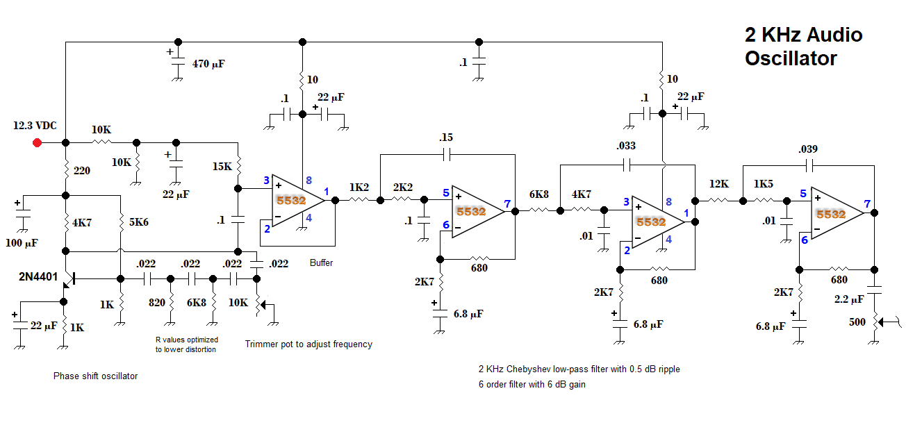
Above — Schematic of 1 of my 1 KHz oscillators. I've got several. This 1 features a tweakable center frequency and uses a split +/- 15 VDC supply. The signal gets attenuated 12 dB by the buffer and then goes into 6-8 poles of Chebyshev 1% ripple low-pass filters. This proves the lowest distortion oscillator in my world.
I wanted an AF oscillator for 2 and 4 KHz for radio AF work. I built several and will present 3.
Digital 2.04 and 4.1 KHz Crystal Oscillator
Above — Schematic of a digital crystal oscillator. A small bag of 32.768 KHz watch crystals lies in my parts bins. Using a 74HC393, I divided by 8 or 16 to get the target frequencies. I'll only show the 4.1 KHz filter and outputs.
At ~4.1 KHz, when I applied a 74HC14 inverter as a buffer, a problem arose:
Above — Shocked, I toiled and toiled to fix this problem. However, nothing worked except to remove the inverter buffer I initially used as shown in the 2 KHz arm above. Somehow the 74HC14 buffer was oscillating and gave me much grief. I made a low-pass filter with both L-C and op-amps; although you could do it all with just op-amps.
Here's my first op-amp filter for the 4 KHz arm:
Above — The op-amp filter that followed the Pi L-C filter.
Above —Feeling dissatisfied with the outcome, I went back to my design computer.
Above — I took the time to design a far more "serious" filter. What a lot of parts!
Above — OK. Wow. That did the trick. Then I decided the digital filter offered too much work and sought to test out phase shift AF oscillators; something, I've never really experimented with.
Phase Shift Oscillators for ~2 and 4 KHz
I wanted to combine a 2 plus 4 KHz into 1 metal box. First up: the 2 KHz oscillator and outcomes.
Above — The 2 KHz low distortion AF oscillator. I tried 1 tweak in the phase shift: a 10K trimmer. Ultimately you've must get a 180 degrees RC phase shift, however, the 10K pot offered some frequency tweaking, and to a small extent, could lower the harmonic distortion. It's important that you set your RC networks with the transistor connected to the buffer you plan to use. Different buffers may change the frequency and distortion characteristics slightly.
I hand picked my resistor values in the phase shift network
and got a 2 KHz oscillator with the 2nd harmonic about 27 dB down from
the
fundamental. Then I applied the low-pass filters.
Above — FFT of the 2 KHz oscillator output. I ran low-pass filters with 6 dB gain after the phase-shift oscillator. The worst harmonic was 65 dB down. It's OK.
Next comes the 4 KHz oscillator:
Above — The 4 KHz oscillator schematic. I experimented with the three RC filter networks that provide the 180 degree phase shift by making the resistors 5K trimmer pots. By tweaking the trimmer pots while looking at an FFT, I made an oscillator with the 2nd harmonic down about 38 dB. This seems really good compared to other phase shift oscillators that I built.
Without these trimmers, results will vary and the 2nd harmonic might otherwise only lie between 22 and 28 dB down. I found that parts tolerances, transistor current, the feedback capacitor value & stray capacitance affect oscillator frequency and distortion characteristics in phase shift oscillators.
Above — FFT of the 4 KHz raw oscillator into a 10 K resistor load. By tweaking the trimmers in the RC phase shift networked, I lowered distortion while viewing the output in an FFT.
Above — FFT of the entire 4 KHz oscillator chain. The worst harmonic (third) is 65 dB down
Above — The 2 and 4 KHz oscillator circuits built Ugly style and mounted in a re-purposed Hammond chassis.
Above —Front view of the two frequency AF test oscillator. This box used to hold an FM receiver and I kept the original drilled holes for the pots and RCA output jacks so it looks bit off kilter.
References
I've already mentioned Audio Power Amplifier Design, 6th edition, however, I also recommend 2 of other Doug Self books: Small Signal Design & The Design of Active Crossovers. This book trio will put your audio design work on the evidence-informed bleeding edge.
Above — A trifecta of great audio design text books.
Above — I got this book for my birthday this year. What a great addition to my library.
Thermal Tracking
The VBE multiplier used to bias the finals into Class B should be thermally connected to your finals so all the PN junctions track. I didn't bother for the aforementioned maximum 2 Watt amplifiers, but strictly adhere to the rule for power amps rated > 2 Watts.
Above — I opened up a broken Phoenix Gold car audio PA to observe how professionals make AF PAs. This 50 W amplifier seems to offer separate BJT and FET power output stages. On the right hand side you can see 2 aluminum plates screwed onto the power transistors to thermally connect them to the main enclosure. I removed the cover plates on the left hand side.
The entire aluminum enclosure is a heat sink with fins and such. You can see lots of polyester and polypropylene film/foil capacitors & metal film resistors in the signal path.
Above — I removed the cover plate to expose the TO-92 VBE multiplier transistor between a set of ST brand TIP power transistors. Those finals are 15 Amp, 60 volt, 90W BJTs. The cover plate thermally coupled the VBE multiplier BJT to the complimentary finals.
Conclusion
I hope I've shown that good, stable AF power amps are easy to make and well compliments the RF and digital work we perform in modern radio design + building. Cheers!