Lab Notes from Transistor Radios

I like making simple component-level radios. This Fall, I rekindled my love for making transistor radios and hope to slowly blog some circuits and fun. I'm warning you now — these circuits hearken the 1970s and 80s, SSD, EMRFD, old issues of Ham Radio and other stuff that require no coding skills.
For the Ham 40 meter band, I thought about employing an Si5351 for the synthesizer -- naw. While this chip poses a great choice, I wanted something a little more organic. If you go the Si5351 route, I recommend you consider the offerings by EtherKit. Jason toiled to improve the Arduino code library for this and perhaps you might support his future efforts?

[Section One — PLL Board]

Above —PLL Board Schematic. I built this whole project employing Ugly Construction.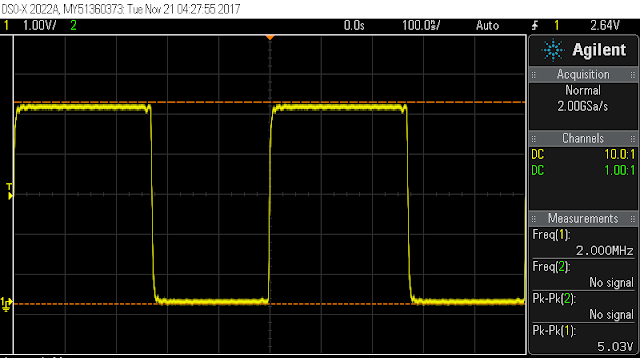

Above — Reference oscillator output. I built the 2 MHz crystal reference oscillator in a familiar Pierce circuit with an 74HC14. This hex inverter with Schmitt-trigger inputs makes a fabulous reference oscillator as seen above.

Above — DSO tracing of the 2 MHz reference divided by 13 in the 74HC193 4-bit synchronous counter.
The internal 4-bit WORD gets programmed by pins 9, 10,1 and 15. By default, all 4 pins are set HIGH. Three N-channel MOSFETs locally switch the appropriate pins to ground according to a front panel 5-position switch. This avoids the usual 4 toggle switches you might otherwise use.
For divide by 12, two steering diodes get employed without the 2K2 current-limiting resistors seen on the other switch positions. Each diodes' forward voltage drop limits the MOSFET gate drive current to ~ 1 mA which is about the current limit offered by the 2K2 resistor in the other switch positions.
The output of the 4-bit counter goes to Pin 3 of a phase-frequency detector built with a pair of 74HC74s. The other 74HC74 clock input (Pin 11) is driven by a 74HC00 buffer which takes the low frequency, sine wave output of the offset mixer and squares it to proper CMOS voltage levels.

Above — The 74HC00 signal squarer in my DSO when tested with a 7.04 MHz signal generator.
With no AC input signal, a CMOS squarer may oscillate somewhere between between ~2 and 70 MHz. My 5 volt 74HC00 DC supply is bypassed from AF to HF and the signal path input is also decoupled and bypassed with the 51 Ω / 470pF network.
For the PLL board, it's literally test as you go. For example, build the 2 MHz Pierce oscillator and look at its output. Then use that output to test the 4-bit counter. Any old bench sine wave oscillator from AF to HF will test the 74HC00 squarer. For the 2 remaining NAND gates: Ground the input pins of one gate while using the other gate to reset pins 1 and 13 in your phase/frequency detector.
I stuck with the classic, low-noise, OP-27 for the loop filter. You'll find the OP-27 in PLL circuits published decades ago. While we enjoy lower noise op-amps today, I got them for low cost long ago and they impart some nostalgia on my bench -- and the OP-27 is still a great part.
Since the VCO operates over a very narrow bandwidth [ hopefully 7.00 - 7.065 MHz ], you can filter the loop well. The 1K2 loop dampening resistor posed critical, so I employed a 1% part in that slot. The critical dampening resistance value in my loop was ~ 1170 to 1188 Ω. If I went below that resistance, the feedback loop goes into spasm and oscillates. A 5% 1K2 resistor might not cut it! Hence, a 1K5 Ω 5% part might be a better choice if you don't have a 1% 1K2 Ω resistor in stock.
For the op-amp filter, two, small, 63v, polyester 1 µF caps were placed in parallel since I lacked a 2.2 µF capacitor. Above ~ 80 KHz, the op-amp loop filter = a third order filter. At low frequencies it functions as a first order filter.
The filter allows the PLL to locks quickly and filters well. The output of the main VCO looks good for a home brew PLL system.

[Section Two — VCO]

Above — The VCO schematic. This VCO provides 3 output ports: main, offset mixer and a port to connect a frequency counter. A frequency counter proves essential, since this style of synthesizer uses a VXO with non-linear tuning; plus frequency overlap or gaps may occur across different divisions of the reference oscillator.
The oscillator and 1 buffer run on a AF low-pass filtered 8 volt DC supply. Any ripple on your oscillator's DC supply can pump the VCO and cause noise modulation.
Two outputs from the PNP Colpitts oscillator get lightly AC-coupled to an NPN buffer that I forgot to label. Its 39 ohm collector resistor provides a low-amplitude signal which is further boosted by Q3 which drives a common base amp (Q4) to prevent any of the frequency counter's digital noise from reaching the main oscillator.
The emitter of the unlabelled NPN buffer stage functions as a normal emitter follower. I ran 9 mA emitter current to preserve the main oscillator signal fidelity. This signal goes to an output port that connects to 1 of the offset mixer's input ports.

The main output circuitry takes signal tapped from the tank inductor L1. I tapped about 2/3 down and could have tapped it lower. In honesty, I was too lazy to rewind the L1 toroid, so I employed a 2.7p coupling cap to provide some low-level signal to Q5 without having to run high current to prevent further distortion of the VCO signal. A FET source current of 8.45 mA preserved the VCO signal fidelity and provides good drive for the final feedback amp.
My initial feedback amp transistor Q6 choice was a 2N2222A. I ran a target 23-24 mA to help achieve a stage output impedance of 50 Ω and raised the *51 Ω emitter resistor shown to 75 Ω to get this. Without a heat sink, the 2N2222a ran at 39-40 degrees C. Rather than make a heat sink, I stuck in a 2SC1971 and changed the emitter resistor to 51 Ω as shown in the schematic. I targeted ~23 mA emitter current.
This BJT runs at 28.7 degrees C and won't run away. The 2SC1971 I used was probably 1 of those cheap bootleg or counterfeit transistors as it cost < 40 cents with free shipping on eBay a few years ago.
I find these "probably bootleg" transistors work OK for HF projects. I've got some original,very old Mitsubishi 2SC1971s in my parts collection reserved for VHF amps + drivers and they cost a fortune now.

Above — A DSO capture of the unfiltered output from the 2SC1971 feedback amplifier (Q6) during some early experiments with attenuation on its output.

Above — An early DSO capture of the frequency counter output in yellow and the main VCO output in green with the low-pass filtered soldered in, but not the 6 dB pad.

Above — Final FBA version into my DSO. I wanted an output close to 10 dBm so I can get ~7 dBm outputs from a quadrature hybrid coupler for use in single signal DC receivers if so desired.

Above — VCO board on my test bench. I soldered a 100K pot with 12.3 VDC supply, so that I could apply reverse DC voltage to the varactors and manually tune the VCO to test its function. Most importantly, this allows you to choose the correct tank inductor and fixed capacitor values.

Above — VCO board on my test bench. As shown, I've got 4.86 volts manually applied to the varactors. I applied 3 back-to-back varactors, plus the small 47 p tank coupling capacitor to allow enough VCO tuning range with the lowest pk-pk AC voltage possible on the varactors to potentially reduce VCO phase noise.
When you connect the varactors to the VCO, tweak the small 5-30p trimmer cap to get phase lock. Switch off the power. Then after 4-5 seconds, switch back on the12 VDC. If your VCO does not phase lock, tweak the trimmer cap some more and repeat. You can connect your voltmeter right to the PLL output to monitor the DC voltage.
My circuit captures and locks the VCO after switching it off and then on with 3.9 volts DC measured on the PLL output with the VXO set to its lowest frequency + the 4-bit counter set to divide by 11. It's then set and forget. Once set, the VCO locks perfectly every time and it stays on the set frequency for days.
[Section Three — Offset Mixer]
 Above — Offset mixer schematic.
 In old CB radio synthesizers, engineers often used a single BJT as an offset mixer (usually they ran 1 for TX and another 1 for RX). To prevent mixer output from leaking out its AC and DC ports, we may do 2 things: well filter the DC going to the BJT -- plus run common-base amps on the 2 BJT mixer inputs to provide reverse isolation for the mixer board input ports.
The VCO and VXO ports get the same common-base amp. An active low-pass (ripple filter), plus some serious decoupling + HF to VHF bypass filter the DC power line. The mixer output gets a simple, but stout, pi low-pass filter. The shunt 560 Ω resistor loads the output to stabilize the output signal + boost filtration.

Above — DSO capture with 10X probe at the output of the 1 µF capacitor. At this point the only filtration is provided by the 1n capacitor shunt to ground, so you still see some mixer products.

Above — DSO capture with 10X probe at the output of the pi low-pass filter. You've filtered it enough when it looks like a sine wave at the correct offset output frequency. I tested it with the project VXO and a bench signal generator.
[Section Four — VXO]
We require a VXO that tunes the VCO from 7.0 to 7.065 MHz. I had some HC49-S style 28.4 MHz crystals and hoped to divided them by 4 -- and get enough frequency swing to tune my desired VCO range. I failed here! The crystals on hand proved terrible and would not pull as far as I'd hoped without compromising my desired less than 1 Hertz VXO temperature drift fluctuation.
I tried them in a super VXO fashion + varied the inductance and such but could not get a fully meshed to fully open tuning capacitor swing over 10 KHz with a divide by 4. In my collection, I found an air variable capacitor that offered more range, but alas it suffered backlash and when I mounted it in my enclosure the Bakelite support material cracked and crumbled rendering it garbage.
I hope to get some different 28.8 MHz crystals and derive the tuning range I initially calculated and hoped to achieve. I will also try to find an air variable capacitor with a lower minimum capacitance like the 1 that broke. Perhaps it was foolhardy to chose a divide by 4 scheme? We'll see.

Above — VXO schematic. The single hex inverter buffer might not be needed, however, I've got lots of CMOS logic to use up and more years behind me than ahead.
Final synthesizer tuning range = 7.007 to 7.065 MHz with some gaps as follows:
Final synthesizer tuning range = 7.007 to 7.065 MHz with some gaps as follows:
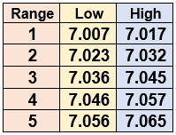
The VXO tunes from 7.189152 to 7.19702 MHz. As mentioned, Ill work on the VXO to remove the gaps in ranges 1, 2 and 3 -- and hopefully get down close to 7.00 MHz.
Limiting the VXO range to only that what's needed improves the synthesizer tuning resolution.
[Section Five — Photos]

Above — All 4 boards were built in re-purposed Hammond boxes. A PIC-based counter sits on top of the offset mixer. I build modular gear and this allows modification and fosters experimentation. When I build a final transistor radio receiver, I plan to place the offset mixer, PLL circuitry and VXO on the same board inside the radio with some shielding. My VCOs always go in a RF tight container. A 0.0033 µF feed through capacitor connects the VCO varactors to the outside world.
Making this project I learned much and like my VCO + mixer, the sublime loop filter and also avoiding toggle switches by running local MOSFET switches. I've already extended the MOSFET switching technique in a more complex PLL for a scratch UHF synthesizer.

Above — All 4 boards on my bench 

Above — Main VCO output in a DSO.
[Section Six — Miscellany]


Above — Cascading two 4-bit counters yields division by 1 to 255. If you were to place all 8 switches on a front panel, we would place the left counter's switches to the right of the 240 weight switches so that we could program it in a more "humanly logical" fashion.
It's great fun to play with old school digital circuitry such as these CMOS chips. I've got the whole series of HC74 synchronous and asynchronous counters in my parts bins.

Above — 3 edge-triggered phase and frequency detectors using D flip flop(s). I normally employ Figure A with active filtering. The op-amp filter boosts the DC output signal up in voltage which may help improve VCO phase noise and stability.
Figure B employs a charge pump. You'll see diodes or transistors used in charge pumps -- often in PLL circuits within ICOM, Yaesu and other brand-name radios.
Compared to the Exclusive OR phase detector ( in the 4046 etc.), edge-triggered phase + frequency detectors exhibit a greater linear tuning range, plus better capture, lock and tracking characteristics. Both types may be effected by input signal duty cycle. 50% proves best.